AMD unveils Instinct MI300X GPU and MI300A APU, claims up to 1.6X lead over Nvidia’s competing GPUs

(Image credit: AMD)
AMD launched its Instinct MI300X AI accelerator and the Instinct MI300A, the world’s first data center APU, during its Advancing AI event here in San Jose, California, as it looks to capitalize on the booming generative AI and HPC market. AMD forged its MI300 lineup using the most advanced production technologies ever pressed into mass production, employing new techniques like its ‘3.5D’ packaging to produce two multi-chip behemoths that it says provide Nvidia-beating performance in a wide range of AI workloads. AMD isn’t sharing pricing for its new exotic silicon, but the products are now shipping to a wide range of OEM partners.
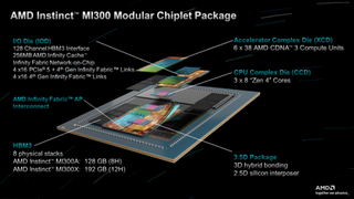
The Instinct MI300 is a game-changing design - the data center APU blends a total of 13 chiplets, many of them 3D-stacked, to create a chip with twenty-four Zen 4 CPU cores fused with a CDNA 3 graphics engine and eight stacks of HBM3. Overall, the chip weighs in with 153 billion transistors, making it the largest chip AMD has ever made. AMD claims this chip delivers up to 4X more performance than Nvidia’s H100 GPUs in some workloads and touts that it has twice the performance per watt.
AMD says its Instinct MI300X GPU delivers up to 1.6X more performance than the Nidia H100 in AI inference workloads and offers similar performance in training work, thus providing the industry with a sorely needed high-performance alternative to Nvidia’s GPUs. Additionally, these accelerators come with more than twice the HBM3 memory capacity than Nvidia’s GPUs — an incredible 192 GB apiece — enabling its MI300X platforms to support more than twice the number of LLMs per system as well as running larger models than Nvidia’s H100 HGX.
AMD Instinct MI300X
The MI300X represents the pinnacle of AMD’s chiplet-based design methodology, melding eight 12Hi stacks of HBM3 memory with eight 3D-stacked 5nm CDNA 3 GPU chiplets, dubbed XCD, on four underlying 6nm I/O dies that are connected using AMD’s now-mature hybrid bonding technique.

